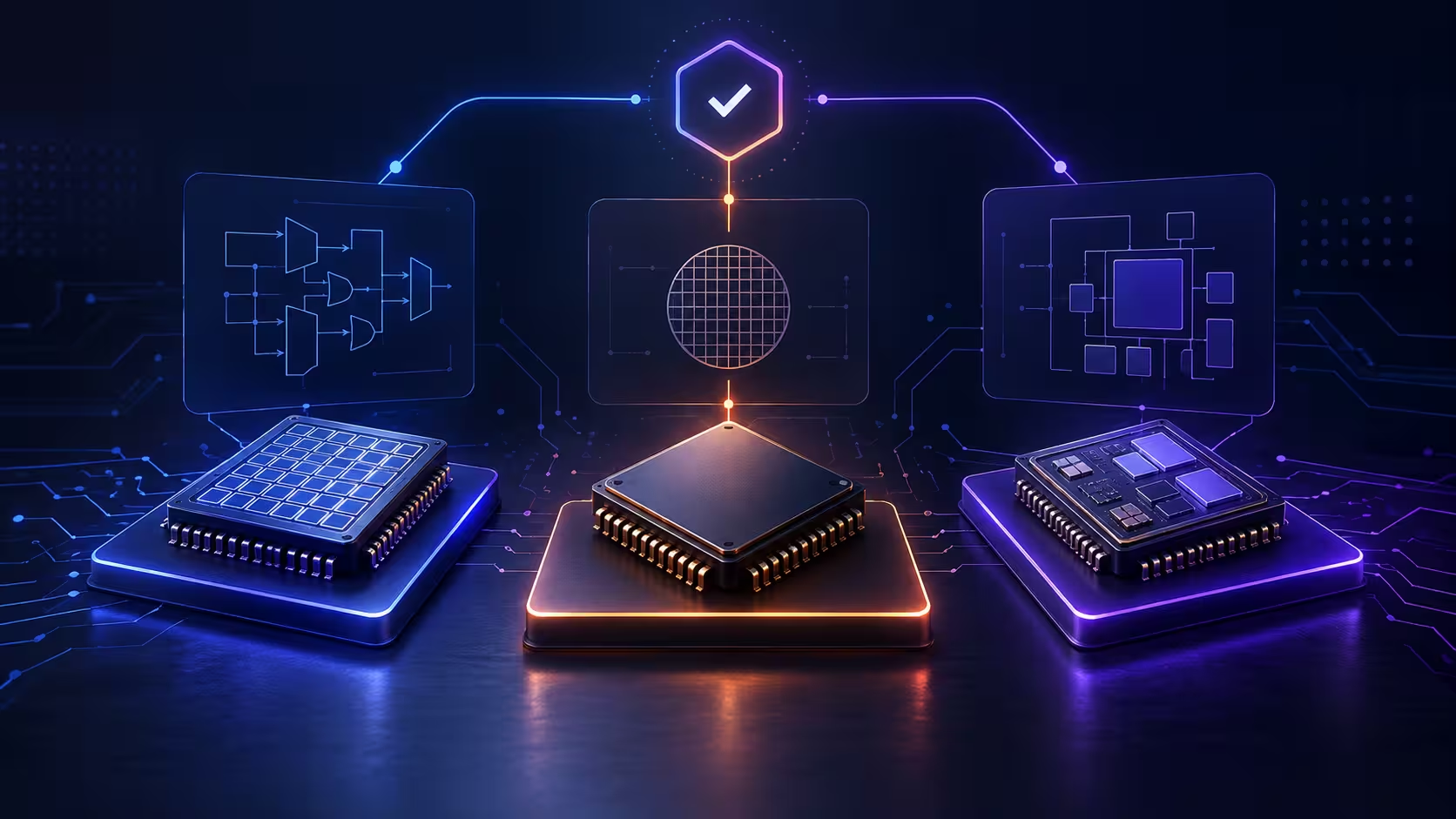
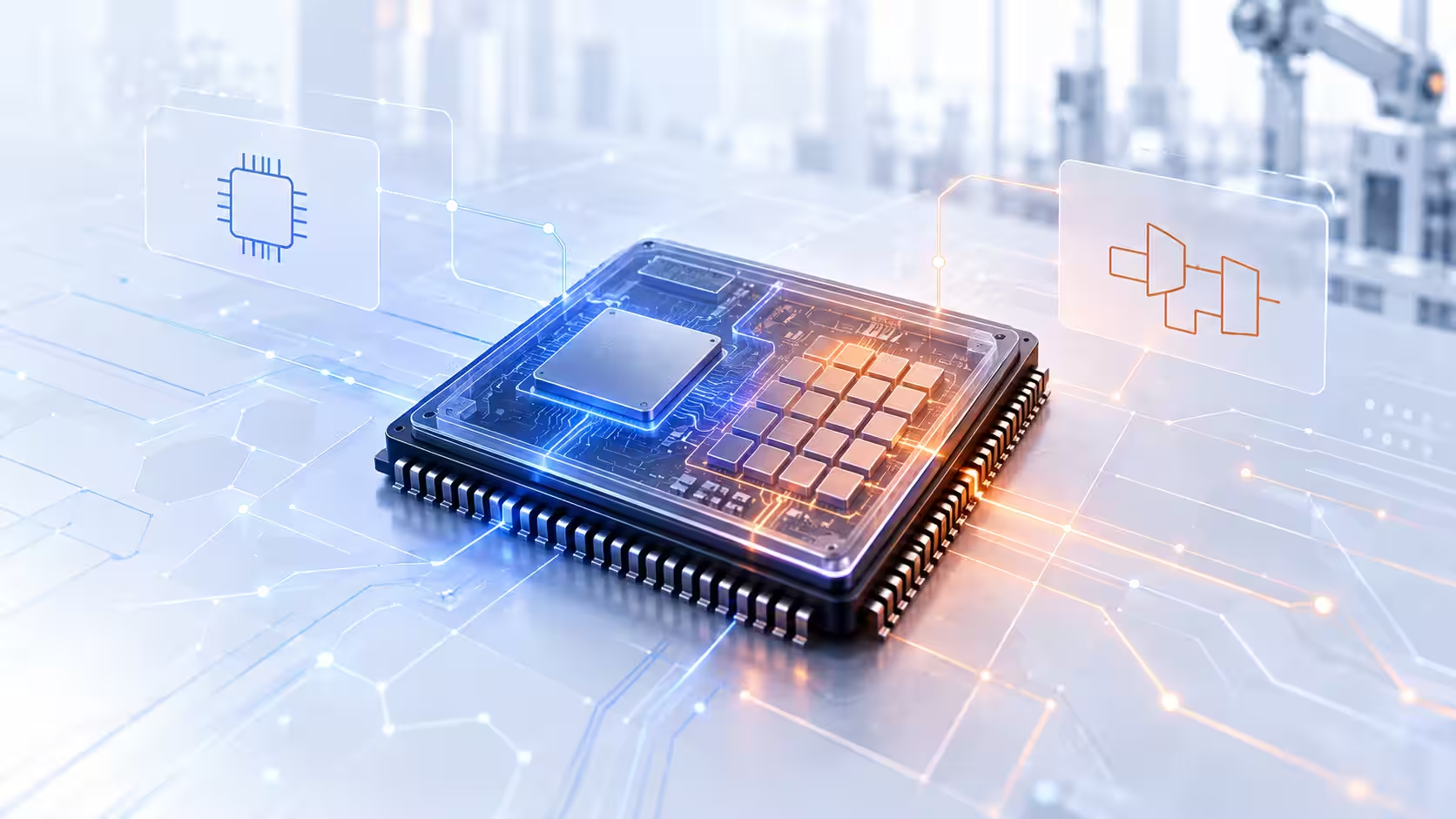
A SoC FPGA puts processor cores and programmable logic on a single chip, two functions on the same device instead of two separate parts on a board. This has been the market direction for roughly a decade: most current parts are hybrids rather than plain FPGAs. As Adam Szychulec, Head of Hardware / Embedded at InTechHouse, puts it, an FPGA used to be an FPGA; today you get ARM cores you can run Linux on, the fabric, often an integrated GPU, and peripherals for fast interfaces, all on one die.
A SoC FPGA puts processor cores and programmable logic on a single chip: two functions, one device, rather than a processor and an FPGA connected across a circuit board. Merging both functions into one device also ties their lifecycles together, a factor that matters when planning for FPGA obsolescence and mid-life upgrades.
That combination has been the direction of the FPGA market for roughly a decade, and most current parts sold today are hybrids of this kind rather than plain, processor-free FPGAs. Today's devices typically add ARM cores capable of running Linux, the fabric itself, often an integrated GPU, and peripherals built for fast, standard interfaces, all on one chip.
This guide covers what the term actually means, how work splits between processor and fabric, where the combination earns its place, and where to find a team that has shipped systems built on it.
"System on chip" on its own has become close to meaningless, and that is worth saying before using the term again.
In general use, SoCs integrate complete systems, a processor, a memory controller, peripherals, sometimes graphics, that would once have needed multiple separate chips on a board. That is why the phone in your pocket, a general purpose application processor and a basic microcontroller are all, technically, systems on chip. The category is too wide to describe anything specific on its own.
The narrower thing this article is actually about is programmable logic on the same die as the processor. That is what "SoC FPGA" means here, and it is the term worth using instead of bare "SoC" from this point on.
The main difference against traditional FPGAs comes down to one thing: where the processor lives.
On a traditional FPGA, a processor had to sit beside the device on the board as a separate chip, or be built inside the fabric itself as a soft core, at the cost of logic resources that would otherwise go to the application. On a SoC FPGA, the processor is hard silicon on the same die as the fabric, connected by high bandwidth on-chip interconnect rather than by traces across a board.
What that actually contains matters to an architect. Zynq UltraScale+, for example, has fabric, graphics capability and two distinct processor types: Cortex-A cores for application software, and Cortex-R cores for real-time work. An application core running Linux next to a real-time core next to programmable fabric, all on one die, is a different design conversation from "a CPU plus an FPGA" wired together on a board. Vendor and third-party IP cores cover most of the standard interfaces on these devices, which is what makes design reuse practical.
An application specific integrated circuit is custom silicon commissioned for one product: it carries non recurring engineering costs and a mask set before a single working part exists, which is why the decision is framed against production volume, and why low volume products rarely reach it.
A SoC FPGA gives a design team an integrated processor-plus-fabric system without that upfront commitment, at the cost of a higher per-unit price and, unlike an ASIC, never quite as optimized for the one function it runs. The full decision between the three is covered in a dedicated guide.
Integration is a mechanical argument, not a marketing adjective, so it is worth explaining what it actually buys a design.
Moving the processor onto the same die as the fabric removes the board traces that would otherwise sit between them, which cuts latency and the power spent driving signals across external interfaces. One device instead of two also means fewer components, simpler power management, and one less connection that can fail, which is where the reliability argument actually comes from, rather than from the silicon being inherently more dependable.
Worth being honest about the other side: a SoC FPGA is not low-power in absolute terms, and it is a poor fit for a battery powered device compared with a simple microcontroller doing the same job. The power efficiency case here is relative, against a two-chip solution doing the same work, not an absolute claim about low power operation on its own.
Check FPGA vs microcontroller guide.
This is the part that distinguishes a real answer from a generic explainer: a method with a worked judgement behind it, not a rule of thumb.
The operating system and the control flow run on the processor. Work that must be parallelised, large data volumes, image processing, signal processing, goes to the fabric instead.
"You put the operating system on the processor, and then the tasks that need parallelising, processing large volumes of data, image, signals, or where you simply need a lot of flexibility in the system for future development, or unusual interface configurations. Then these are very good solutions, combining the advantages of FPGAs and processors. Of course there are certain disadvantages that come with it too."
Adam Szychulec, Head of Hardware / Embedded, InTechHouse
Not every heavy computation belongs in the fabric side of that split. An FFT, for instance, computes better in the processor, worth stating plainly because it proves this partitioning rule was actually applied to real designs rather than recited from a textbook.
The flexibility argument is stronger on a SoC than on a plain FPGA specifically because of this split: resources are often left spare in the fabric so functions can be added later without a PCB change, hardware-level functions rather than a firmware update, while the processor side is still updated in software on its own. Space and aerospace customers do this on purpose.
Check our FPGA hardware acceleration guide.
Where this combination earns its place: environments working with different kinds of data at once, video, telemetry, sensor data; parallel processing of large volumes within a short time; unusual interface configurations a standard processor cannot offer; and flexibility for future development without a board respin.
More broadly, these parts also appear in motor control and industrial drives, instrumentation, consumer electronics and IoT devices, wherever a design needs a general-purpose processor and dedicated parallel logic in the same product.
"Adaptive SoC" is AMD's current marketing name for this class of device, worth knowing if you are searching vendor material directly, though it is a branding term rather than the framework this article uses.
The wider landscape: AMD/Xilinx offers Zynq and Zynq UltraScale+; comparable families exist at Intel/Altera; Microchip has its own SoC FPGA line; Lattice builds comparable parts on RISC-V. Choosing between them is its own decision. Check Choosing an FPGA vendor and family guide.
InTechHouse has delivered several Zynq and Zynq UltraScale+ systems for telecom, aerospace and oil & gas customers, working day to day in Vivado, Vitis, Quartus, Lattice Radiant and Lattice Diamond across FPGA and SoC design generally.
Worth stating plainly: these solutions combine the advantages of both worlds, and there are certain disadvantages too. The one worth naming is the tooling. Many of these tools work the way they work, with plenty of bugs and in constant development, and the workflow splits between the logic itself and how software gets loaded onto the device, and with which tools. That tooling experience is a second competence layer on top of the hardware design itself, and it is a real part of what a customer is buying from a team that has already climbed that curve.
Not sure whether your project needs a SoC FPGA or a plain FPGA? Request an FPGA architecture assessment.
Not sure where to start? We work with companies at every stage, from early ideas to enterprise-level builds. A 30-minute call can save you months of guesswork.
A plain FPGA is programmable logic alone, with a processor sitting separately on the board if the design needs one. A SoC FPGA integrates processor cores and programmable logic on the same chip instead.
Zynq is AMD/Xilinx's SoC FPGA family. Zynq-7000 is a device within it, and yes, it is an FPGA in the sense that it contains programmable logic fabric alongside ARM processor cores.
A CPU is a single processing component. A system on chip integrates that processor with memory controllers, peripherals and other components on one die, which is why bare "SoC" says little on its own.
An ASIC is custom silicon fixed at manufacture for one function; an FPGA is reconfigurable logic; a SoC FPGA integrates reconfigurable logic with hard processor cores on one chip. The full trade-off is covered in a dedicated guide.
PYNQ is an open-source project that puts a Python development environment on top of Zynq devices. Zynq is the underlying silicon; PYNQ is a software layer built for it.
A more complex development flow than a plain processor, vendor tooling that carries real bugs and is in constant development, and two competences needed instead of one: hardware design and processor-side software.
No. A Raspberry Pi is a board built around an application processor system on chip with no programmable logic on it. A SoC FPGA adds reconfigurable fabric alongside the processor instead.
Damian Ledziński, PhD Eng., is an Applied Artificial Intelligence Expert and an Assistant Professor at Bydgoszcz University of Science and Technology. He has over 15 years of academic, research, software-engineering, and technology-development experience.
His work focuses on applying artificial intelligence, machine learning, deep neural networks, and data science to complex real-world systems. His principal research and engineering interests include autonomous unmanned aerial vehicles, drone navigation and swarm intelligence, biomedical engineering, medical signal and image analysis, predictive modeling, industrial IoT, and intelligent water-management systems.
Damian has contributed to multidisciplinary R&D initiatives including AI-assisted medical diagnostics, a Polish ventilator prototype, autonomous indoor drone systems for warehouse inventory, AI-supported water-consumption analysis, virtual medical assistants, and intelligent systems combining embedded devices with machine-learning models.
He is the author or co-author of more than 30 scientific publications. His work has appeared in international scientific publications covering artificial intelligence, biomedical engineering, signal analysis, autonomous systems, environmental monitoring, and data-driven infrastructure.
Damian is a co-creator of academic programs in Engineering in Medicine, AI in Medicine, and Data Science at Bydgoszcz University of Science and Technology. He combines scientific research with hands-on implementation, translating experimental AI methods into deployable technology. He writes about applied AI, machine learning, predictive analytics, autonomous UAV systems, AI in medicine, biomedical signal processing, industrial IoT, and intelligent models in real-world systems.
Damian Ledziński's academic profiles:
https://wtie.pbs.edu.pl/pl/pracownik/damian-ledzinski
https://www.researchgate.net/profile/Damian-Ledzinski
https://scholar.google.pl/citations?user=AlQpPB0AAAAJ&hl=pl
https://ludzie.nauka.gov.pl/ln/profiles/DN6pHXU6KZm/publications/f83a8833-6060-4fae-8628-3dbf57661394
This initial conversation is focused on understanding your product, technical challenges, and constraints.
No sales pitch - just a practical discussion with experienced engineers.
Share a few details about your product and context. We’ll review the information and suggest the most appropriate next step.