.avif)
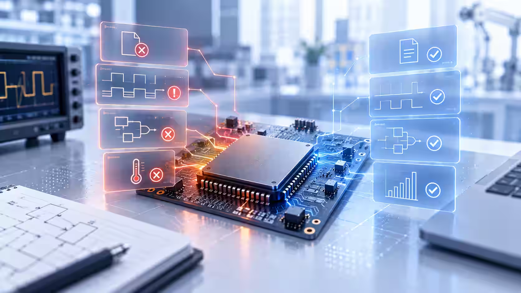
"In an FPGA you move to another level, where you have to start thinking that these things happen in parallel. And when you write code, you are not writing instructions for a processor. You are really writing hardware in code. You create gates, you create an electronic circuit by writing code."
Adam Szychulec, Head of Hardware / Embedded, InTechHouse
Nearly every mistake in this article follows from that sentence: thinking sequentially about hardware that is actually concurrent. This guide covers the failure modes that keep recurring across the industry, not in one team, and what actually catches them before hardware. These are the two failures we see most in FPGA design, and this article explains why they happen and how they get caught.
Every mistake below traces back to the same starting point: FPGA design is hardware design, not software running on different rules. That mindset shift is usually forced by a project, typically at the moment a team discovers when an MCU is no longer enough for its latency or throughput targets.
Writing code for an FPGA does not produce instructions for a processor to execute one after another. It describes logic, a circuit, that exists all at once, in parallel, on silicon. The habits that work well in software, loops, sequential thinking, "this runs, then that runs", carry hidden assumptions that do not hold once code is describing hardware instead of controlling it.
This article covers the failure modes that follow from that gap: what causes them, why they recur across experienced teams rather than only beginners, and what actually catches them before a design reaches hardware.
A loop in software runs over time, one iteration after another. The same construct written in RTL can unroll into that many physical copies of the same logic, consuming logic elements the author never budgeted for. A long expression packed into a single clocked process can become a long combinational path between two clock edges, one the design was never going to meet timing on.
A short fragment makes the shift concrete:
verilog
always @(posedge clk) begin
  sum <= a + b + c + d;
end
This describes a register, sum, and the adder logic feeding it, built from real gates on the device. It is not an instruction executed on a schedule. If a, b, c and d are wide buses, that single line is real adder hardware sized to match, evaluated every clock edge, whether or not the result is needed that cycle.
The consequences a reader will recognise from their own project: resource usage that balloons past what the design should need, timing that will not close because a path like this sits between two registers with no room to spare, and functional blocks that behave differently on real hardware than the author's mental model predicted while writing the code.
The same habit shows up in a smaller, sharper form: leaving a branch out of an if-else chain, or a case out of a case statement, in a block meant to describe combinational logic. In software, an unhandled branch just does nothing. In RTL, it tells the synthesis tool to hold the previous value when that condition is not met, which infers a latch rather than the plain combinational logic the author actually intended. It is one of the fastest ways to turn a design that looks correct into one with timing and behaviour nobody planned for.
Clock domain crossing, CDC, is the highest-volume search term behind this article, and it earns that volume: it is one of the two failures experienced FPGA engineers actually run into, not a beginner error engineers grow out of.
A clock domain crossing happens when a signal generated in one clock domain is sampled in another. Most real designs have more than one clock domain by necessity, not carelessness: an external interface running its own system clock, a transceiver, a slower peripheral, a processor core running at a different clock frequency from the fabric around it. Wherever two of those meet, a signal has to cross from one clock domain into another, and that crossing is where the risk sits.
Not every crossing carries the same risk. Where two clocks have a known, fixed phase and frequency relationship, derived from the same source rather than truly independent of each other, the crossing is a synchronous one and can sometimes be handled with simpler, more targeted techniques than a fully asynchronous crossing needs. Treating every crossing as equally dangerous, or equally safe, is itself a source of mistakes in both directions.
When a receiving flip-flop is clocked at the exact moment its input is changing, it can enter a metastable state and resolve unpredictably, settling on a value that is neither the old one nor the new one. The underlying requirement is simple to state and easy to miss in practice: source data has to stay stable for long enough before the receiving clock edge samples it, and data loss follows directly if it does not. What makes this fail commercially rather than just theoretically: the failure is intermittent, often invisible in functional simulation, and so it tends to surface late, on hardware, at a customer, or in a batch that behaves differently from the one before it.
For a single-bit signal, a two-flop synchroniser is the standard fix. For a bus of multiple bits, synchronising each bit separately is not safe, because the bits can arrive on different clock edges and produce a combined value that never actually existed on the sending side; a handshake, or an asynchronous FIFO, is the correct approach instead. The underlying design rule is architectural: decide deliberately where clock domains meet and cross them in one place, rather than treating CDC as something to patch in after the fact.
Asked what the most common FPGA mistakes are, Adam Szychulec reaches first for transitions between different clock domains, not as an item on a list but as something he has actually run into on real projects. A CDC bug can pass functional simulation cleanly, meet every stated timing constraint, and still fail once it reaches silicon, which is exactly why it is expensive rather than merely common. Clock gating is a related trap worth naming in passing, and CDC checking itself is a distinct analysis from ordinary synthesis and timing closure, not something either of those catches automatically.
The second failure Adam names from his own experience, stated without softening: a design works in simulation and then does not work in hardware. It is a recurring event across the industry, not an anomaly limited to any one team.
The textbook reasons behind it are worth understanding precisely. Functional simulation checks a design's behaviour against a testbench; it cannot, by itself, prove timing behaviour on the actual device. A testbench often never modelled real interface timing or real-world signal behaviour in the first place, which is exactly why writing a properly robust testbench, one that exercises edge cases and realistic interface timing rather than just the happy path, is critical for catching bugs before they ever reach hardware. And missing or incorrect timing constraints let the implementation tools sign off on a design that was never actually checked against the timing it will run at.
The practical consequence for a buyer: simulation coverage is not evidence of a working product, and on-target testing, running the design on real hardware, is a phase with real time and budget attached to it, not a formality tacked on at the end. Check FPGA design flow.
The critical path is the longest path between two clock edges in a design, where logic delay plus routing delay together determine the arrival time at the next register, and that arrival time sets the maximum clock frequency the whole design can run at. Put precisely, in the terms a timing report actually uses: the critical path is the path with the most negative slack, slack being the margin, or shortfall, between when a signal is required to arrive and when it actually does. A path that fails setup is not simply "a slow design". It is one register placed too far from another, with too much logic, and not enough margin, sitting between them.
The mistake is treating timing closure as something the implementation tools handle automatically at the end of the flow. In practice, under-specified timing constraints surface here as an unbuildable design, and the fixes run in a fairly fixed order a practitioner recognises: correct the constraints first, then restructure the RTL itself, pipelining the path or breaking up the logic, then influence placement, and only after all of that consider changing the device. Pipelining specifically works by reducing the number of logic levels a signal has to pass through in a single clock cycle, trading an extra register stage, and an extra cycle of latency, for a shorter path between registers. Where the operation itself is arithmetic, using the device's designated arithmetic units, dedicated multiplier or DSP blocks rather than logic built from general-purpose fabric, can also help meet a constraint that generic logic never will. The tools optimise against exactly what you declare to them. An unconstrained path is not a fast path. It is simply an unchecked one, and that single distinction is the most useful thing in this section.
Filling a device close to its limit is a mistake with a cost that can actually be priced. A design running at very high utilisation is harder to route, harder to close timing on, and leaves nothing spare for the next feature, so that next feature becomes a device change, and a board change along with it. Intel's own Quartus documentation puts a number on it directly: utilization of 95 percent or more of a device's resources can be difficult to fit, regardless of how well the design itself is written (Intel, 2021). The practitioner's rule is simple to state: pick a device that meets today's requirements and leaves real headroom, not the smallest part that technically fits. Check our guide on Choosing an FPGA vendor and family.
Two related habits push utilisation and timing risk up at the same time. Gating a clock with local combinational logic instead of a dedicated clock-enable structure introduces clock skew and glitches that a clean clock tree does not have, and it is a difficult problem to diagnose after the fact because it looks like an ordinary timing failure until someone traces it back to the clock network itself. Asynchronous resets on every register, used by default rather than by decision, consume more resources than a synchronous or synchronised reset strategy and can introduce their own timing violations around reset recovery and removal, on top of routing congestion from resetting more of the device than the design actually needs to.
On any complex design, the architecture decision comes before RTL, not after: what runs on a processor and what belongs in fabric, where the clock domains actually meet, which functional blocks are separable and testable on their own. Design partitioning done late is design partitioning done twice, once badly and once properly. HLS tools are worth one honest mention here: they raise the level of abstraction a designer works at and can be the right tool for an algorithmic block, but they do not remove the need to think about hardware, pipelining and memory access, they just change how that thinking gets expressed in code.
Check What is a SoC FPGA.
An article about FPGA mistakes that blames only the engineer is a lecture. One that names the tools as a contributing factor was written by someone who has actually used them. Tool maturity also belongs in the earlier decision about offloading algorithms to FPGA, because synthesis and timing tools shape what the logic can realistically deliver.
Many of these tools work the way they work: plenty of bugs, in constant development, and what works reliably at one vendor does not necessarily work the same way at another. The actionable conclusion is not a complaint, it is a fact worth planning around: vendor-specific experience is what shortens this gap, and it is a distinct competence from general HDL skill. AMD/Xilinx, Intel/Altera, Lattice and Microchip each have their own tooling quirks in this respect, and finding out which ones apply to your project on your own time is expensive. Check How to choose an FPGA design company guide.
This is not a side note. It is the actual reason the failure modes above recur across the whole industry rather than inside one particular team. Getting started in FPGA design is hard, the source material and teaching resources are thin, and it requires a real change in how someone thinks about writing code. Most embedded engineers never touch the area at all, including, by Adam's own account, most of his own department, who are strong on processor-based work rather than fabric.
The device manufacturers themselves are the main source of usable knowledge. There are a few good books, mostly written outside Poland. Structured training is scarce: Adam names Doulos as training that exists in the market, and says that when he looked for FPGA training in Poland there was very little available, so the practical path is to look abroad and work much of it out directly. For a reader trying to build this skill, vendor documentation and named training providers like Doulos are a useful starting point, not a marketing mention.
What actually catches these mistakes is process, not individual cleverness. Clock domain crossings get treated as an architectural decision, reviewed deliberately rather than left to be found later. Timing constraints get written from day one of a project, not bolted on once the design already exists. And testing on the actual target hardware starts early, rather than being saved for the end of the schedule.
The more honest version of "how experienced teams avoid this" is that a customer's own evidence regime catches a great deal of it. Beyond the design simply working, a regulated customer typically requires it to be testable, repeatably tested with evidence, and written to their own code standard, and InTechHouse has delivered FPGA logic that met exactly those requirements, including safety-integrity requirements, on a rail project. Even inside an electronics team, most engineers can work around FPGA design entirely for their whole career, which is one reason this kind of work tends to get contracted out rather than built as an in-house function.
Want a second pair of eyes on an FPGA design before it goes to hardware? Request an FPGA architecture assessment.
Not sure where to start? We work with companies at every stage, from early ideas to enterprise-level builds. A 30-minute call can save you months of guesswork.
Metastability on single-bit crossings, incoherent data on buses synchronised bit by bit instead of as a group, and intermittent failures that pass simulation cleanly and then fail on real hardware. All three share the same root cause: a signal crossing between clock domains without a proper synchronisation structure.
A request signal and an acknowledge signal cross in opposite directions between the two clock domains, each passing through its own synchroniser, with the data held stable until the receiving side confirms it has been captured safely. This avoids the risk of sampling a bus mid-change.
Static analysis that checks a design's source code for clock domain crossings and verifies each one uses a recognised synchronisation structure, run before simulation and well before hardware. It catches a category of bug that functional simulation is not built to find.
A setup violation is a signal that does not arrive at a register before the next clock edge; a hold violation is one that changes too soon after that edge instead. Both mean the design cannot reliably run at the clock frequency it was built for until the underlying path is fixed.
Because simulation proves behaviour against a testbench, not timing on real silicon. A testbench that never modelled real interface timing, or timing constraints that were missing or wrong, both let a design pass simulation and synthesis while still failing once it actually runs on the target device.
Harder than it looks to an engineer coming from software, for a specific reason: it requires thinking in parallel hardware rather than sequential instructions, and the material available to learn it from is thin compared with mainstream software education.
A higher unit cost, more power draw than a microcontroller for the same function, longer build cycles, and a smaller pool of engineers who can actually do the work well. Check our FPGA vs microcontroller guide.
Because a generic integer or a default-width type is sized far wider than most counters or state variables actually need, the synthesis tool has to build logic elements and routing fabric to match that unnecessary width. Sizing a signal to the number of bits it actually needs, an unsigned type with an explicit range rather than a bare integer, avoids paying for width the design never uses.
Because a mechanical or noisy external input can toggle several times within a single clock period as it settles, and a state machine sampling that signal directly will see false transitions it was never designed to handle. Debouncing the input before it reaches any state logic is what prevents those false triggers.
Poor structure and inconsistent naming, more than any single technical bug. A design where signal names do not describe their purpose, and where related logic is not grouped in a way another engineer can follow, is slower to debug and easier to modify incorrectly, even when every individual line of RTL is technically correct.
Tomasz Andrysiak, DSc, PhD, is a Expert and a Professor at Bydgoszcz University of Science and Technology. He has more than 30 years of academic, research, R&D, and technology-implementation experience in artificial intelligence, computational intelligence, signal processing, anomaly detection, cybersecurity, and complex information systems.
His research focuses on machine-learning and computational-intelligence methods for analyzing signals, time series, network traffic, industrial data, and multimodal datasets. He specializes in anomaly and failure detection, predictive modeling, intelligent monitoring, critical-infrastructure security, smart metering, biomedical signal analysis, and the practical deployment of AI in industrial and public-sector systems.
Tomasz is the author or co-author of more than 75 scientific publications, including papers published in internationally recognized journals and conference proceedings indexed by Web of Science and Scopus. His research has covered network anomaly detection, cybersecurity of critical infrastructure, ECG signal analysis, machine learning, smart water networks, telecommunications, and intelligent industrial systems.
He has led and contributed to national and European R&D programs focused on cyber situational awareness, critical-infrastructure resilience, autonomous systems, Big Data, intelligent water management, blockchain-based transaction platforms, and industrial AI. He leads industrial-doctorate projects involving AI-based CMDB automation and machine-learning methods for knowledge discovery in Big Data.
Tomasz is an IEEE Senior Member and has served as an elected member of the Commission of Informatics and Automation of the Polish Academy of Sciences, Poznań Branch. He has participated in scientific committees and journal boards, supervised doctoral research, reviewed publications for international journals, and co-authored patents and patent applications related to signal detection and LoRa-based ECG monitoring. He writes about industrial AI, machine learning, anomaly detection, predictive analytics, cybersecurity, signal processing, time-series analysis, and intelligent infrastructure.
Tomasz Andrysiak's academic profiles:
https://link.springer.com/chapter/10.1007/978-3-642-32384-3_28
https://www.researchgate.net/profile/Tomasz-Andrysiak
https://scholar.google.com/citations?user=RHW7zx4AAAAJ&hl=pl
https://dblp.org/pid/41/6793.html
https://radon.nauka.gov.pl/dane/profil/6FFA1E51186802ECFFB49644209B5BE0EBD68C55
https://pbs.edu.pl/pl/pracownik/tomasz-andrysiak
https://www.youtube.com/watch?v=6e1GTqT5czM
This initial conversation is focused on understanding your product, technical challenges, and constraints.
No sales pitch - just a practical discussion with experienced engineers.
Share a few details about your product and context. We’ll review the information and suggest the most appropriate next step.