


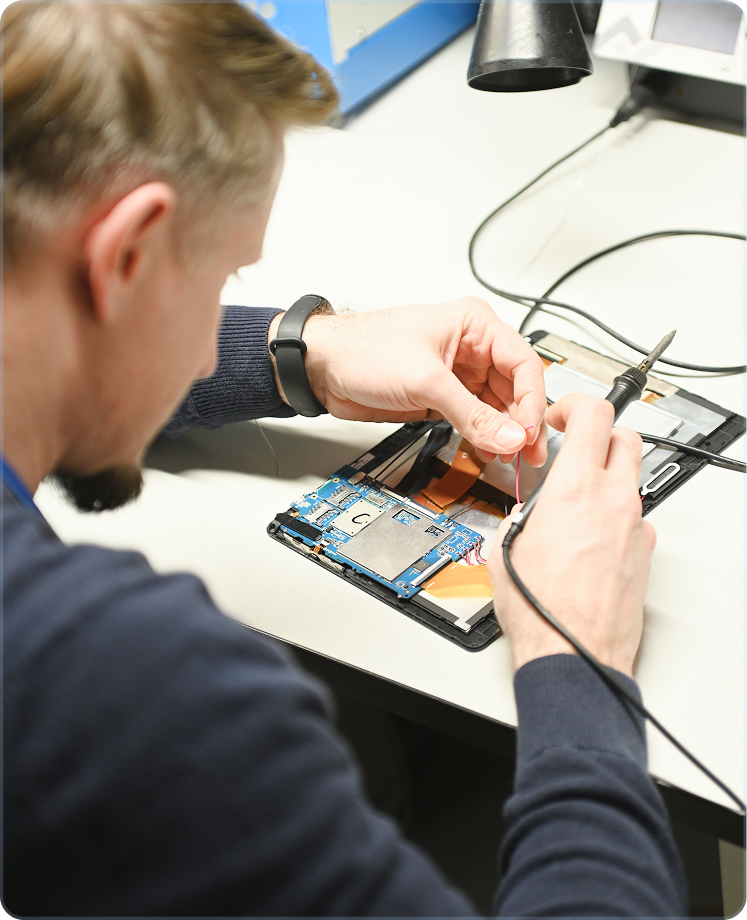
FPGA Design & High-Performance Embedded Systems
We design high-performance embedded systems using FPGA and SoC architectures where CPU-based solutions reach their limits, enabling parallel processing, low latency and deterministic execution in demanding environments.


Measured impact on high-performance system architecture
Our FPGA-based systems remove CPU bottlenecks, enabling predictable performance under high data load and strict timing constraints.
How we design high-performance FPGA systems
FPGA performance comes from architecture, not optimization after implementation. Early decisions define throughput, latency and system behaviour.
Parallel processing by design
- Data paths are designed as parallel pipelines, not sequential execution flows
- Processing stages are mapped to hardware to eliminate CPU bottlenecks
- Throughput and latency are defined at architecture level
System-level integration
- FPGA, CPU and memory are designed as a single system, not separate components
- High-speed interfaces and data movement are aligned with real bandwidth requirements
- Hardware acceleration is integrated with embedded software and control layers
What defines a high-performance FPGA system
System performance is determined by how processing pipelines, data movement and timing are structured at the architecture level.
Data flow is structured to maximise parallel processing and eliminate sequential bottlenecks across the system.
Signal paths and processing stages are aligned to maintain timing accuracy across multiple channels and interfaces.
System design allows adding new features or processing stages without redesigning the hardware platform.
Use Cases
We design high-precision FPGA IP cores and programmable logic architectures for aerospace systems that demand exact timing, predictable execution, and long-term reliability. Our work focuses on delivering architectures that maintain consistent performance under strict operational constraints, supporting mission-critical functions where accuracy and stability are essential.


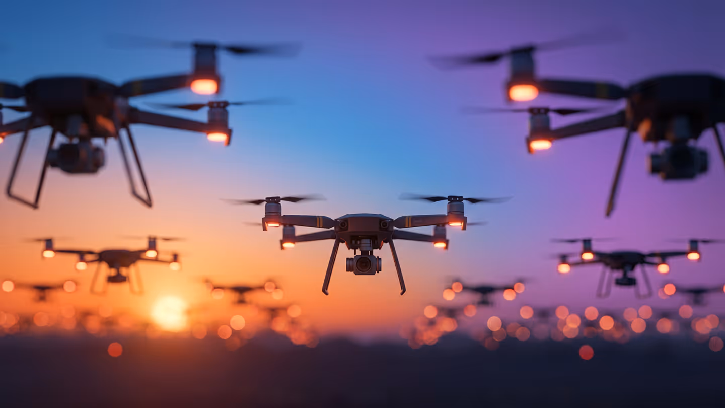
We design FPGA/PLD-based real-time video processing systems for multispectral UAV platforms that require precise image acquisition, parallel sensor data processing, and high-speed data transmission to ground control. The architecture is built for continuous operation in mission-critical environments, delivering stable performance and predictable behaviour.

We design high-reliability aerospace electronics platforms that combine FPGA-enabled SoC architectures with multilayer PCB design, enabling advanced processing flexibility and future adaptability. Programmable logic allows new functionality to be introduced without hardware redesign, reducing lifecycle costs and supporting long-term system evolution.
We executed a full HDL migration for a subsea communication module, porting legacy FPGA and modem logic to modern hardware using VHDL and Verilog. This approach extended the operational lifecycle of safety-critical infrastructure without requiring a full system redesign, while maintaining compatibility with existing system constraints and performance requirements.


Industries We Serve
Our engineering capabilities are deployed across regulated, mission-critical and industrial sectors.
Subsea electronics, downhole systems and harsh-environment hardware for offshore and onshore operations.
FPGA engineering for real-time signal processing, video processing and hardware acceleration in aerospace systems.
FPGA-based signal processing and hardware acceleration for high-performance industrial data acquisition systems.
FAQs
If you have additional questions or would like to discuss your requirements, feel free to get in touch with our team.
Field programmable gate arrays are integrated circuits that can be configured after manufacture to implement custom digital logic in hardware rather than software. Where a processor executes instructions sequentially, an FPGA fabric runs multiple operations in true parallel, which is what makes FPGA-based embedded systems the right choice for applications where timing, throughput, or determinism requirements exceed what a conventional processor can deliver.
Real-time processing is the most common driver. Applications that need to act on data within a fixed, guaranteed time window, with no tolerance for the latency variation that operating systems and processor pipelines introduce, benefit from logic implemented directly in the FPGA fabric. The processing happens in hardware, at clock speed, without software overhead.
Digital signal processing is another area where FPGAs are well suited. Filtering, transformation, and analysis of high-bandwidth signal streams can be implemented in custom logic that processes data as it arrives rather than buffering it for sequential handling. This is particularly relevant in communications, radar, imaging, and audio applications where the data rates involved would overwhelm a software-based approach.
High-speed interfaces are where the specific capabilities of FPGA embedded systems become most visible. FPGAs are commonly used to implement and manage interfaces that require precise timing and high throughput, including Fiber Channel for storage networking, HD-SDI for professional video, and QDR II for high-bandwidth memory access. These are the kinds of high-performance solutions that general-purpose processors handle poorly or not at all, because the interface timing requirements have to be met in hardware.
The reconfigurability of field programmable gate arrays also means that the same physical hardware can be updated to support protocol changes, new interface standards, or revised processing requirements without replacing the silicon, which extends the useful life of the embedded system and reduces the cost of adapting to changing requirements.
When the task requires parallel processing, deterministic timing, or custom logic that a fixed processor architecture cannot accommodate, an FPGA is the right choice. A microcontroller or CPU executes instructions one at a time, in sequence, which means that tasks with hard real-time requirements or high data throughput demands will eventually hit a ceiling that software optimisation cannot overcome.
Parallel processing is the defining advantage. An FPGA implements multiple operations simultaneously in hardware, so a design that needs to process several data streams at once, handle multiple high-speed interfaces in parallel, or perform DSP operations on incoming data without buffering can do all of that concurrently rather than time-slicing across a single core.
Deterministic timing is the other key factor. When a system needs to respond to an event within a fixed, guaranteed window, every time, the non-determinism introduced by operating system scheduling, cache behaviour, and pipeline stalls in a conventional processor becomes a problem. Logic implemented in an FPGA responds at clock speed, with timing that is defined by the design rather than by runtime conditions.
Custom logic covers the cases where no standard processor peripheral or interface meets the requirement. Clock generation, custom communication protocols, non-standard memory interfaces, and application-specific DSP pipelines can all be implemented in the FPGA fabric directly, rather than worked around in software.
FPGAs are also not limited to pure hardware logic. Soft-core processors can be instantiated within the FPGA fabric, and many modern FPGAs include hard processor cores alongside the programmable logic. This means a single device can run embedded software for the parts of the application that benefit from it, while custom hardware logic handles the tasks that require determinism or parallel throughput. The combination gives designers the flexibility of a software-programmable system with the performance headroom of dedicated hardware where it matters most.
FPGA development follows a structured flow that moves from requirements through to a deployed, integrated system. Each stage builds on the previous one, and the decisions made early in the process have a direct impact on how straightforward verification and deployment turn out to be.
Requirements definition establishes what the FPGA needs to do: the interfaces it must support, the processing it must perform, the timing constraints it must meet, and the platform it will be deployed on. Getting this right at the start prevents the kind of scope changes that are expensive to accommodate once RTL work is underway.
RTL design and FPGA code development is where the logic is implemented. Register transfer level design describes the hardware behaviour that will be synthesised into the FPGA fabric, covering data paths, control logic, interface handling, and timing constraints. This is the core engineering work of FPGA development, and the quality of the RTL directly determines how the implemented design performs.
IP development and integration allows proven, pre-verified logic blocks to be incorporated into the design rather than implemented from scratch. Standard IP cores for common interfaces, communication protocols, memory controllers, and DSP functions cut development time significantly and reduce verification risk. Where standard IP does not meet the requirement, custom IP is developed and documented for reuse.
Verification confirms that the design behaves as specified before it is deployed to hardware. Simulation, formal verification, and hardware-in-the-loop testing are used to find and resolve issues at the stage where they are least expensive to fix.
Deployment covers programming the FPGA and integrating it into the wider system. FPGAs can be configured on power-up by a microprocessor, which is the standard approach for production systems where the configuration bitstream is loaded from non-volatile storage each time the device starts. Firmware development and system integration are part of the full delivery, ensuring that the FPGA logic and the software running alongside it implement the complete product behaviour rather than just the hardware component of it.
In most FPGA-based embedded systems, the processor and the programmable logic handle different parts of the workload, and the quality of the integration between them determines how well the system performs as a whole.
The processor, whether a hard core integrated into the FPGA device or a soft-core instantiated in the fabric, handles control flow, system management, communication with external interfaces, and the parts of the application that benefit from flexible, software-based implementation. The FPGA fabric handles the tasks that require deterministic timing, parallel throughput, or custom hardware logic that a processor cannot deliver efficiently on its own.
The handoff between hardware logic and firmware is where the integration design matters most. Data moving between the processor and the FPGA fabric passes through defined interfaces, typically memory-mapped registers, shared memory regions, or dedicated bus connections such as AXI. The firmware needs to know exactly what the hardware logic expects to receive, what it will produce, and under what timing conditions. Hardware logic that is not designed with the firmware interface in mind creates integration problems that are difficult to resolve without changes to both sides.
Firmware development for FPGA-based systems therefore requires close coordination with the RTL design. The software team needs visibility into the hardware behaviour, and the hardware team needs to understand what the firmware will ask the logic to do. This is not a handoff between two separate workstreams but a collaborative process where decisions on one side regularly affect the other.
Machine learning workloads follow the same pattern. Where an FPGA is used to accelerate inference, the fabric implements the compute-intensive parts of the model while firmware handles data preparation, result interpretation, and integration with the rest of the system. Getting the boundary between hardware acceleration and software control right is what determines whether the combined system meets its performance and latency targets.
Most of the risk in FPGA projects concentrates in a small number of well-understood areas. Knowing where those areas are, and planning for them, is what separates projects that close on schedule from those that stall in the final stages of development.
Timing closure is consistently where FPGA development takes longer than expected. Meeting the timing constraints of a complex design, across all paths, all corners, and all operating conditions, requires disciplined RTL coding practices from the start and iterative work between synthesis and place-and-route. Designs that accumulate timing debt through the development process tend to face a difficult closure effort at the end, when schedule pressure is highest.
Verification is the other area where effort is frequently underestimated. An FPGA implements custom hardware, and hardware bugs are harder to find and fix than software bugs. Thorough simulation, formal verification where applicable, and structured hardware-in-the-loop testing are what catch issues before board bring-up, where the cost and time of finding them is significantly higher. Design-for-test practices, building in visibility and controllability from the RTL stage, make board bring-up faster and reduce the time spent diagnosing problems on real hardware.
Power and thermal limits affect reliability and constrain what the FPGA fabric can do within the physical envelope of the design. Power efficiency is not just a battery life concern. Thermal limits affect reliability and determine what cooling approach the enclosure needs to support. Both need to be analysed during development, not discovered during testing.
Regulatory compliance adds a further layer of complexity in sectors where FPGA-based systems are subject to functional safety standards, electromagnetic compatibility requirements, or documentation and traceability obligations. Meeting these regulatory standards requires that the development process itself is structured appropriately, not just that the finished design passes the relevant tests.
Performance optimisation in FPGA-based systems comes down to making the best use of what the fabric offers, while staying within the power and thermal envelope the hardware can sustain.
Parallelism is the primary lever. Where a processor handles operations sequentially, the FPGA fabric can implement multiple processing elements running simultaneously, each handling a portion of the workload in the same clock cycle. Designing the RTL to exploit this parallelism, rather than describing logic that behaves like sequential software, is what allows FPGA-based systems to achieve throughput that fixed processor architectures cannot match. The degree of parallelism that is practical depends on the available fabric resources and the power budget, so these constraints shape the architecture from the start.
Clock generation and distribution have a direct impact on both performance and reliability. Careful clock generation, using dedicated clock management resources within the FPGA, ensures that logic operates at the correct frequency with stable timing margins across process, voltage, and temperature variation. Poor clock design introduces timing uncertainty that limits the maximum operating frequency and can cause intermittent failures that are difficult to reproduce and diagnose.
Power and thermal optimisation is a key factor in FPGA design, and one that affects both reliability and cost. Reducing dynamic power consumption through clock gating, logic optimisation, and careful management of switching activity lowers the thermal load on the device and the system around it. A design that runs cooler requires less aggressive cooling, which reduces enclosure cost and improves long-term reliability. Power efficiency also directly affects operating cost in deployed systems, which compounds over the lifetime of the product.
The combined effect of these optimisations is high-performance solutions that deliver the required throughput and latency at lower costs than less considered approaches. Getting performance, power efficiency, and cost into the right balance is the central engineering challenge of FPGA design, and it is one that has to be addressed at the architecture level before RTL work begins.
Performance optimisation in FPGA-based systems comes down to making the best use of what the fabric offers, while staying within the power and thermal envelope the hardware can sustain.
Parallelism is the primary lever. Where a processor handles operations sequentially, the FPGA fabric can implement multiple processing elements running simultaneously, each handling a portion of the workload in the same clock cycle. Designing the RTL to exploit this parallelism, rather than describing logic that behaves like sequential software, is what allows FPGA-based systems to achieve throughput that fixed processor architectures cannot match. The degree of parallelism that is practical depends on the available fabric resources and the power budget, so these constraints shape the architecture from the start.
Clock generation and distribution have a direct impact on performance and reliability. Careful clock generation, using dedicated clock management resources within the FPGA, ensures that logic operates at the correct frequency with stable timing margins across process, voltage, and temperature variation. Poor clock design introduces timing uncertainty that limits the maximum operating frequency and can cause intermittent failures that are difficult to reproduce and diagnose.
Power and thermal optimisation is a key factor in FPGA design, and one that affects both reliability and cost. Reducing dynamic power consumption, through clock gating, logic optimisation, and careful management of switching activity, lowers the thermal load on the device and the system around it. A design that runs cooler requires less aggressive cooling, which reduces enclosure cost and improves long-term reliability. Power efficiency also directly affects operating cost in deployed systems, which compounds over the lifetime of the product.
The combined effect of these optimisations is high-performance solutions that deliver the required throughput and latency at lower costs than less considered approaches. Getting performance, power efficiency, and cost into the right balance is the central engineering challenge of FPGA design, and it is one that has to be addressed at the architecture level before RTL work begins.
FPGA-based systems are used across a broad range of industries where real-time processing, deterministic timing, or high-speed interface handling are requirements that standard processor-based designs cannot meet.
In high-frequency trading, FPGAs process market data and execute trading logic with latency measured in nanoseconds. The time advantage over software-based systems running on conventional processors is significant enough that FPGA-based designs have become standard infrastructure in firms where execution speed is a direct competitive factor.
Telecommunications infrastructure, including 5G cell tower hardware and high-capacity networking equipment, relies on FPGAs to handle the signal processing, protocol implementation, and data routing that the throughput demands of modern networks require. The reconfigurability of field programmable gate arrays is also an advantage here, since protocol standards evolve and hardware that can be updated in the field has a longer useful life than fixed-function devices.
Automotive applications include the LiDAR and radar processing systems used in autonomous vehicles and advanced driver assistance. These devices generate high volumes of sensor data that need to be processed in real time to produce the situational awareness outputs that safe vehicle operation depends on. Machine learning inference at the edge is increasingly part of this processing pipeline, and FPGAs are used to accelerate those workloads where latency and power constraints rule out cloud-based approaches.
Aerospace and defence represent some of the most demanding FPGA applications. Radar systems, satellite communications hardware, and the Joint Tactical Radio System are among the programmes that depend on FPGA-based designs for signal processing, encryption, and protocol handling in environments where reliability, security, and the ability to update deployed hardware in the field are all critical requirements. These are sectors where the combination of high performance, design flexibility, and long operational life makes FPGA-based systems the standard rather than the exception.
InTechHouse works with the leading FPGA technology providers, with primary experience across Xilinx, now part of AMD, and Altera, which covers the devices used in the large majority of commercial and defence FPGA programmes.
Xilinx and AMD devices span from cost-optimised FPGAs for high-volume applications through to high-capacity devices for demanding signal processing and data centre workloads. The Xilinx portfolio includes programmable SoCs that combine ARM processor cores with FPGA fabric on a single device, which simplifies system architecture and reduces board area for designs that need both software flexibility and hardware acceleration.
Altera devices cover a similarly broad range, with the Stratix 10 family representing the high end of the portfolio for applications that require maximum fabric capacity, high-speed transceivers, and integrated security features. The Stratix 10 includes a Secure Device Manager that handles device authentication, key storage, and secure boot, which is relevant for designs deployed in environments where the integrity of the FPGA configuration needs to be protected against tampering or reverse engineering.
Partial reconfiguration is supported across both vendor families and allows sections of the FPGA fabric to be updated while the rest of the device continues operating. This capability is valuable in systems that need to adapt their hardware functionality at runtime, whether to switch between processing modes, update protocol implementations, or load different accelerator configurations without taking the system offline.
AES encryption of FPGA bitstreams is a standard security measure for designs where the configuration itself represents intellectual property or where loading an unauthorised bitstream would compromise system integrity. Both Xilinx and Altera technologies support bitstream encryption, and InTechHouse incorporates this into FPGA design services for programmes where security is a requirement rather than an option.
Choosing an FPGA design services partner is a decision that affects the entire product lifecycle, not just the initial development phase. The criteria worth evaluating go beyond whether a team can write RTL.
Technical expertise and toolchain familiarity are the starting point. An engineering team that works closely with vendor tools, including Vivado, Quartus, and the associated simulation and verification environments, produces designs that are better optimised and easier to maintain than those developed by teams working around gaps in their toolchain knowledge. The skills required for timing closure, power analysis, and high-speed interface implementation are specific and take time to develop.
Verification methodology is where many FPGA projects accumulate hidden risk. Partners who apply structured, automated verification approaches, including open verification methodology frameworks, catch functional issues before hardware exists rather than during board bring-up. This is one of the clearest indicators of whether a team will deliver a working design on the first silicon or require multiple iterations.
IP ownership should be clearly defined in the contract before work begins. The RTL, testbenches, and documentation produced during an FPGA development programme represent significant value, and ambiguity about who owns what creates problems at exactly the point when the client needs to maintain, extend, or transfer the design.
Design-for-test practices determine how straightforward board bring-up and production testing will be. A partner who builds in visibility and controllability from the RTL stage reduces the time and cost of commissioning hardware significantly.
Long-term FPGA availability is a practical consideration that is easy to overlook during development. Choosing devices with confirmed long-term supply commitments, and working with a partner who tracks vendor roadmaps, prevents the situation where a product requires a costly redesign because the FPGA it was built around has been discontinued.
InTechHouse addresses each of these criteria directly, with an engineering team experienced across the leading vendor toolchains, structured verification practices, clearly defined IP terms, and long-term support built into the delivery model.
Discuss your product with our expert
This initial conversation is focused on understanding your product, technical challenges, and constraints.
No sales pitch - just a practical discussion with experienced engineers.


Share a few details about your product and context. We’ll review the information and suggest the most appropriate next step.