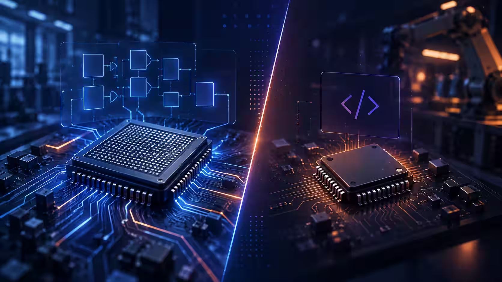
In the world of electronics, two design processes play a crucial role in the development of functional electronic devices: electronic hardware design and PCB (Printed Circuit Board) design. While they are closely related and often overlap under the broader umbrella of pcb hardware design, they involve distinct areas of expertise and focus on different aspects of electronics engineering. Understanding the differences between these two disciplines is essential for hardware designers, engineers, and anyone involved in the development of electronic products, from industrial automation equipment to consumer devices.
In this article, we will introduce the most significant differences between the hardware design process and PCB design, their significance in the development of modern electronic devices, and best practices for optimizing performance, reliability, and production costs. Additionally, we will discuss how these two engineering fields work together, with careful planning at every stage, to ensure functionality and compatibility efficiency in real-world applications.
Hardware design is a multidisciplinary engineering process that involves the creation of electronic circuits, systems, and devices from the ground up. This domain requires a deep understanding of electrical engineering, physics, and material science. Unlike PCB design, which focuses on the physical implementation, hardware design addresses the high-level architecture and logic behind an electronic system. The most essential aspects of hardware design include:
Here's more about hardware development process.

On the other hand, PCB design is a specialized subset of hardware engineering that focuses on translating schematic designs into physical circuit boards that can be manufactured and assembled, and the critical role of PCB design begins exactly at that translation step. It requires a deep understanding of signal integrity, electromagnetic interference (EMI), thermal management, and manufacturability constraints. Unlike hardware design, which involves high-level system architecture and component selection, PCB design is concerned with the practical implementation of electronic circuits in a way that ensures optimal performance and reliability. Before moving to practical implementation, consider the following:
Are you interested in this theme? We encourage you to read the article about the critical role of PCB design.

| Feature | Hardware Design | PCB Design |
| Focus | Conceptual and functional design of the electronic system | Physical layout and interconnections of the components |
| Main Output | Schematic diagrams, component selection, and system architecture | Gerber files, layout designs, and manufacturing-ready PCB blueprints |
| Tools Used | SPICE simulators, circuit design software (e.g., Altium Designer, KiCad, LTspice) | PCB layout software (e.g., Altium Designer, Eagle, OrCAD, KiCad) |
| Involves | Selecting and integrating electronic components, designing circuits, and defining system architecture | Arranging components on the PCB, routing traces, optimizing for manufacturing |
| Considerations | Functionality, performance, power consumption, cost | Signal integrity, thermal management, manufacturability |
The split also shows up in the toolchain. Architecture and simulation work lives in SPICE-class tools, while placement, routing and Gerber output belong to modern PCB design software, and mixing the two roles in one environment is where teams usually lose time.
Most delays come from buying PCB layout when the project still needs architecture and component selection, or the other way round. We scope both layers and tell you where your product really sits.
Find out which scope your project actually needs
Hardware and PCB design is a process that requires not only advanced technical knowledge but also a strategic, step by step approach to optimizing performance, reliability, and production costs. Careful planning at every stage of the hardware design process reduces the risk of costly rework once a board reaches the manufacturer.
"Failing to follow proper design guidelines can lead to costly revisions and performance issues. The best engineers know that rigorous testing and iterative design are non-negotiable."
- underlines Dr. Alan Hayes, Electrical Engineering Professor.
Designing modern and functional devices requires applying proven methodologies to minimize errors and streamline implementation. To ensure a smooth development process, consider these best practices:
Layer count is one of the earliest decisions that binds both disciplines together. Once a board needs dedicated power and ground planes, routing density, impedance control and cost all move at the same time, so the multilayer PCB design guide is worth reading before the stack-up is frozen.
A deep understanding of both hardware design and PCB design is essential for creating cutting-edge electronic devices that are not only functional but also optimized for real-world applications, from industrial automation systems to consumer wireless devices. While the hardware design process establishes the fundamental logic, performance, and component integration, PCB design ensures these concepts are translated into a practical, manufacturable format that meets industry and regulatory standards. As technology continues to evolve, mastering the synergy between these disciplines, with hardware designers and PCB engineers working as one team throughout the process, will remain the most important driver of advancement in electronics engineering.
We are not interested in mediocrity. At InTechHouse, we believe that the future belongs to those who design it. We don’t ask, "Is it possible?" but rather, "How can we make it better?". Our solutions combine innovative thinking, advanced engineering, and experience that translates into real business benefits. We support our clients at every stage - from concept and prototyping to implementation and optimization.
If you want to create the technologies of the future, choose a partner who understands its potential. Schedule a free consultation and give your company the opportunity to grow.
Our engineers own the path from system architecture and component choice through to routed, manufacturable boards, so nothing is lost in the handover between the two disciplines.
Not sure where to start? We work with companies at every stage, from early ideas to enterprise-level builds. A 30-minute call can save you months of guesswork.
PCB layout can start before the hardware design is finished, but only on the parts that are already stable. Board outline, connector positions, mounting holes, stack-up and placement of major components such as the processor, memory and power stages can be defined once the architecture and key parts are fixed. Detailed routing should wait for a reviewed schematic, because late changes to pin assignments or packages force rerouting and often reopen signal integrity work.
PCB design hands over a complete fabrication and assembly package, not just Gerbers. The fabrication side includes Gerber (RS-274X) layers or an intelligent format such as ODB++ or IPC-2581, NC drill files, a fabrication drawing with stack-up, material and impedance requirements, and an IPC netlist for electrical test. The assembly side includes the bill of materials, pick-and-place centroid data, assembly drawings with polarity marks, and instructions for programming or conformal coating.
Whether a product needs separate hardware design and PCB layout engineers depends on board complexity. On simple two- or four-layer boards, one engineer can handle schematic and layout efficiently. Dense high-speed designs with DDR memory, FPGAs or multi-gigabit links usually benefit from a dedicated layout specialist working alongside the circuit designer. The split works only if routing constraints are captured in the EDA tool's constraint manager rather than passed around in emails or meeting notes.
IPC-2221 is the generic standard for printed board design: it covers conductor spacing versus voltage, current-carrying capacity, materials, hole sizes and general layout requirements. IPC-7351 covers land patterns for surface-mount components, defining how pad sizes are derived from component dimensions and tolerances, with most, nominal and least material density levels. Together they help a board pass fabrication and assembly consistently, while product safety standards may still require larger creepage and clearance distances.
DFMEA (Design Failure Mode and Effects Analysis) is a structured review that lists how each part of a design can fail, what effect each failure has, and how likely and detectable it is. In hardware design it is most useful after the schematic is drafted and before layout release, while mitigations such as protection circuits, derating or redundancy are still cheap. Automotive projects usually follow the AIAG and VDA FMEA handbook, and the results feed the verification plan.
Robert Obiała is a Senior Embedded Systems and Hardware Engineer at InTechHouse with over 12 years of hands-on experience in electronic product development. He specializes in embedded hardware design, multilayer PCB development, firmware engineering, EMC compliance, system integration, and troubleshooting complex electronic devices.
Robert works across the complete product development lifecycle - from system architecture and component selection through schematic and PCB design, embedded software development, prototyping, testing, pre-compliance validation, and preparation for production.
His project experience includes FPGA-based onboard computers for the space industry, low-power IoT and telemetry devices, industrial data acquisition systems, UAV payload electronics, power electronics, and embedded hardware and software for advanced optical equipment. He has designed systems based on STM32, ESP32, AVR, ARM, and AMD Xilinx Zynq platforms, using C, C++, Embedded Linux, and communication technologies including Ethernet, CAN, RS-485, SPI, I2C, UART, Wi-Fi, BLE, MQTT, and LTE-M.
Robert holds an Engineer's Degree in Electronics and Telecommunications and has completed specialist training in EMC-aware electronics design. He writes about practical hardware development, embedded systems, PCB design, firmware engineering, EMC testing, FPGA-based architectures, and bringing reliable electronic products from concept to production.
This initial conversation is focused on understanding your product, technical challenges, and constraints.
No sales pitch - just a practical discussion with experienced engineers.
Share a few details about your product and context. We’ll review the information and suggest the most appropriate next step.