
Thermal management is no longer merely a final-stage optimization step in the design process. It is an integral component of the overall engineering workflow. The designer must balance mechanical, electrical, and cost constraints with the requirements for effective heat dissipation. In high-performance electronic devices, the choice of cooling strategy becomes critical. Passive approaches rely on conduction and natural convection, using heat sinks, thermal vias, or copper layers. During active solutions include fans, forced air circulation, and advanced liquid cooling systems.The purpose of this article is to compare passive and active thermal management strategies in high-performance PCB design, taking into account their limitations, application contexts, and impact on long-term system reliability. As Ralph Remsburg, author of Thermal Design of Electronic Equipment, emphasized:
“Reliability is directly related to temperature.”
The analysis will address both engineering considerations and practical design trade-offs. These factors determine the optimal solution based on the specific characteristics of the application, including the material properties and thickness of the pcb substrate.
Need Professional PCB Design Services?
Our design team has over 22 years of experience designing PCBs for automotive, medtech, and IoT industries. We offer comprehensive services – from concept to production.
In PCB assemblies, heat is generated primarily in active components such as MOSFETs, drivers, and FPGA/SoC devices, as well as in power resistors. Additional heat is produced in conductors carrying high currents due to I²R losses, which are directly determined by electrical resistance. It is critical to distinguish between average power and transient power. Short pulses can create localized hot spots even when the average power appears “safe.” Heat is dissipated through three mechanisms:
Thermal design is best described using a thermal resistance network model. RθJC (junction-to-case) determines how much heat is transferred from the semiconductor junction to the package. Meanwhile, RθJA (junction-to-ambient) depends on the PCB stackup, copper distribution, thermal vias, heatsinks, and convection conditions. JEDEC standard JESD51 measurement data show that RθJA values measured on standardized test boards can differ by over 100% compared to real application conditions (JEDEC JESD51 series).A PCB behaves as a layered structure with limited through-thickness thermal conductivity due to dielectric materials. Therefore, thermal paths with low thermal resistance are essential, including copper pours, internal planes, and vertical “chimneys” formed by thermal vias that conduct heat to layers with greater dissipation area. The most common bottlenecks include insufficient thermal contact area beneath the component and discontinuities in copper continuity, such as slots or isolation gaps.They also include excessive Z-axis thermal impedance through the laminate and unintended thermal barriers created by thick solder mask layers over high-power copper regions. In practice, the objective is to control junction temperature and temperature gradients, as these drive solder fatigue, material degradation, and shifts in electrical performance.
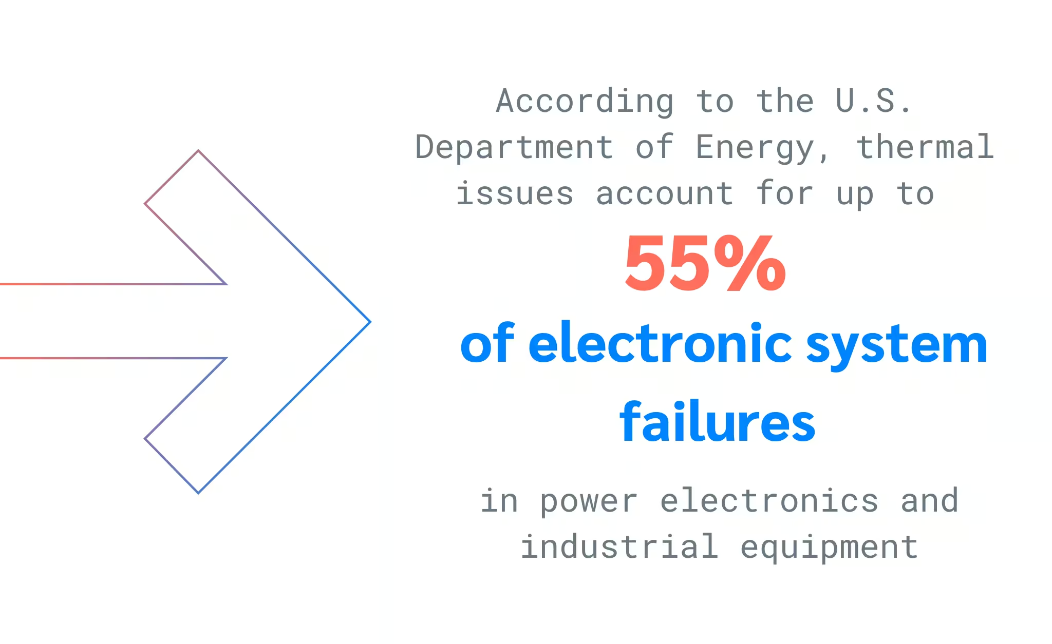
Power density represents a critical design constraint in modern PCBs because it directly determines the requirements imposed on the thermal architecture. It is not merely the ratio of total power to board area, but a local parameter associated with a specific component or functional region. Dr. Yogendra Joshi, a leading researcher in microelectronics cooling, summarized the challenge succinctly:
“The trend toward miniaturization inevitably increases heat flux.”
In practice, two devices dissipating identical power may create entirely different thermal challenges if their heat dissipation area or coupling to the PCB differs.High power density results in concentrated heat flux, increasing the risk of exceeding allowable temperature limits even when the system’s total power is moderate. Particularly sensitive are:
For LEDs specifically, the U.S. Department of Energy reports that lumen maintenance can drop by 10–20% when junction temperature rises from 85°C to 105°C, significantly reducing operational lifetime.An additional factor is the accumulation of multiple heat sources within a confined space. In highly integrated designs, thermal effects are not linear, as mutual heating between components alters the boundary conditions.Therefore, power density analysis should include mapping the spatial distribution of losses and evaluating the maximum heat flux per unit area. It should also verify whether the selected PCB stackup and geometry can dissipate this energy without exceeding temperature limits under both nominal and worst-case operating conditions.If you want to explore the Top 7 Design Rules for High-Speed PCB Layouts, be sure to check here:https://intechhouse.com/blog/top-7-design-rules-for-high-speed-pcb-layouts/
In high-performance PCB designs, the stackup should be treated as a parameterized thermal model whose properties result from cross-sectional geometry, the distribution of functional layers, and their relative spacing. The positioning of power layers with respect to the center of the board thickness is particularly important. Placing them closer to the surface facilitates coupling to a heatsink or enclosure. In contrast, a central position promotes more symmetrical heat distribution but increases the thermal path length to the ambient environment. How does layer positioning influence both thermal resistance and mechanical stability?The number of layers also changes the nature of heat propagation. In a simple four-layer configuration, heat spreading capability is limited to a small number of planes. In eight-layer and higher designs, it is possible to create dedicated “thermal cores,” meaning continuous power planes with high thermal mass that help stabilize short-term overloads and more effectively spread heat across the board area.In multilayer PCBs, effective in-plane thermal conductivity increases significantly when continuous copper planes are present. Research presented at IPC APEX EXPO conferences demonstrates that adding two internal copper planes can reduce peak surface temperature by 10–18°C in high-power modules dissipating 15–20 W.Dielectric thickness is another critical parameter. Thinner layers improve thermal coupling between planes but affect controlled impedance and signal integrity. An asymmetric copper distribution or uneven trace thickness across layers, combined with temperature differences, can generate local stresses and PCB warpage, particularly in applications subject to thermal cycling.The stackup also has mechanical implications. An asymmetric copper distribution combined with temperature differences between layers can generate local stresses and PCB warpage, which is particularly relevant in applications subject to thermal cycling. For this reason, layer design should result from a multi-criteria analysis that integrates thermal, electrical, and mechanical requirements rather than serving merely as an extension of a standard signal-layer configuration.
Discover the Top PCB Design Companies in 2025
Not sure which PCB design partner to choose? We've analyzed and ranked the best companies across the globe based on expertise, technology, quality certifications, and client reviews.
Via stitching strategies under high-power components should create the most continuous thermal conduction path possible from the thermal pad to internal layers and to the opposite side of the board. Vias must not be placed randomly. The array should cover the heat-generating area, and the density must be selected to reduce local thermal resistance without excessively weakening the copper plane. Directly influence on optimal performance:
A larger drill size and thicker copper barrel improve heat conduction, but they increase manufacturing complexity and consume valuable area beneath the component. An overly tight pitch can also raise the risk of etching defects, registration issues, and process variability.In thermal applications, the choice between filled and tented vias is critical. Filled vias reduce solder wicking and improve surface planarity under exposed-pad packages, but they increase cost and introduce process-related risks such as voiding or filler shrinkage. Tented vias are more economical but do not fully eliminate solder loss and may reduce assembly consistency.Under BGAs and power packages, thermal via arrays are commonly implemented, often combined with via-in-pad technology. This requires close coordination with the PCB manufacturer, including consideration of limits on minimum drill diameter, positional tolerances, and filling and planarization requirements. It also requires verification of long-term reliability under thermal cycling, including risks such as copper barrel fatigue, cracking, and potential delamination.
Heat spreading in passive cooling begins at the PCB level with the deliberate use of copper areas exhibiting high thermal conductivity. Copper pours should be designed as continuous heat spreaders with low-impedance coupling to the loss-generating region, minimizing neck-downs and interruptions caused by clearance rules or unnecessary thermal relief patterns. Effective spreading also requires prioritizing large, uninterrupted planes and verifying that no thermal “bottlenecks” are created at transitions between copper regions.When the PCB alone is insufficient, heatsink integration becomes critical. This includes:
In many cases, performance is determined more by the interface than by the heatsink itself. Thermal interface materials (TIMs) reduce microscopic air gaps but introduce their own thermal resistance. An excessively thick layer or insufficient mounting pressure can negate the expected benefit. For this reason, a controlled mechanical tolerance chain must be designed to maintain consistent contact, using springs, torque-limited screws, or retention clips.In fanless enclosures, natural convection requires a system-level approach. Fin orientation, vertical airflow channels, and avoidance of hot-air pockets can be more important than adding extra aluminum mass. Enclosure-level thermal paths, such as through standoffs, mounting plates, or chassis elements, must be continuous and vibration-resistant. The primary advantage of passive cooling is reliability. The absence of moving parts eliminates mechanical failure modes and performance degradation caused by bearing wear. It also reduces sensitivity to dust and lowers acoustic and electromagnetic noise, typically improving parameter stability over the product lifecycle.Passive cooling offers measurable reliability benefits. Field reliability data collected by the U.S. Air Force in electronics maintenance studies indicate that mechanical components such as fans account for up to 20–30% of field-replaceable failures in certain avionics subsystems. Eliminating moving parts reduces failure rate and mean time between failures (MTBF).

Active cooling in PCB systems typically begins with forced convection, but simply adding a fan rarely solves the problem without proper airflow control. Airflow management includes sealing bypass paths, directing air through the most thermally stressed regions, and designing ducts and baffles to minimize recirculation and dead zones. Fan selection should be based on matching the fan curve to the system impedance, which reflects pressure drops across filters, heatsinks, and airflow channels. The key parameter is the operating point. An oversized high-speed fan in a high-impedance system may operate inefficiently, generating noise without delivering proportional airflow gains. Is the airflow path engineered as carefully as the electrical layout?Active cooling introduces additional complexity. Typical axial fans consume between 1W and 10W depending on size and airflow rate. In high-density telecom systems, forced airflow can reduce component temperature by 15–25°C, but at the cost of acoustic noise often exceeding 40–60 dBA.When power density exceeds the limits of air cooling, liquid cooling becomes a viable option. Cold plate integration requires control of flatness, clamping force, and appropriate TIM selection, as well as management of leakage risk and galvanic corrosion within the loop. Thermoelectric coolers (Peltier elements) can locally reduce the board's temperature below ambient, but they introduce significant power overhead and require effective heat removal on the hot side. Otherwise, they may degrade overall thermal performance.The cost of active cooling extends beyond the bill of materials. It includes:
Design must account for failure modes such as fan stoppage, clogged filters, or pump degradation. Redundancy (N+1), tachometric or pressure monitoring, thermal alarms, and safe derating strategies are commonly implemented to prevent cooling failure from causing catastrophic system damage.
Criterion
Passive cooling
Active cooling
Heat dissipation capability
Limited
Significantly higher
Impact on component temperature
Reduction depends on copper area and heatsink size
Typically 15–25°C lower temperatures with forced airflow
Reliability (MTBF)
High
Plus faible
Consommation électrique
Aucune alimentation supplémentaire requise
1 à 10 W (ventilateurs), plus élevé pour les systèmes de refroidissement liquide
Complexité de conception
Plus faible
Plus élevé
Coût total de possession (CTP)
Plus faible
Plus élevé
Les modèles analytiques deviennent insuffisants lorsque la géométrie du système est complexe et que le transfert de chaleur dépend de la convection forcée, de la recirculation et des pertes de charge localisées. Les flux de travail basés sur la CFD sont de plus en plus courants. Une enquête menée par Mentor Graphics (aujourd'hui Siemens EDA) a révélé que plus de 70 % des projets de PCB à haute complexité dans les secteurs de l'aérospatiale et des télécommunications intègrent la simulation thermique avant le prototypage. Dans de tels cas, la CFD n'est pas seulement un outil pour générer des cartes de température visuellement attrayantes. Elle est utilisée pour évaluer quantitativement si, dans une configuration de flux d'air et de boîtier donnée, le système peut maintenir la marge thermique requise. Les conditions aux limites sont critiques :
Tout aussi importante est la modélisation précise des propriétés des matériaux. L'anisotropie des stratifiés, la conductivité effective de l'empilement, la résistance de contact aux interfaces et les paramètres des TIM ne peuvent pas être traités comme des valeurs génériques de fiches techniques, car ils dominent souvent le budget thermique.En pratique, des flux de travail électro-thermiques couplés sont appliqués. Les distributions de pertes de puissance issues de simulations électriques, PI ou SI (ou de données au niveau du circuit intégré) sont introduites dans le modèle CFD. Les champs de température résultants sont ensuite réinjectés pour mettre à jour les paramètres et les pertes dépendant de la température. Cette boucle itérative permet l'identification des points chauds avant le prototypage, grâce à l'analyse de la densité de flux thermique et de la sensibilité aux variations du flux d'air. La confiance dans le modèle nécessite une corrélation avec des mesures empiriques, y compris des thermocouples, la thermographie infrarouge avec contrôle d'émissivité et des capteurs de température embarqués. La CFD devrait guider les itérations de conception, y compris les ajustements des canaux de flux d'air, de la géométrie des dissipateurs thermiques, du placement des composants et de l'empilement. Ces itérations devraient se poursuivre jusqu'à ce que des marges thermiques stables soient atteintes dans des conditions nominales et dans les pires scénarios.
Le choix entre refroidissement passif et actif ne doit pas être traité comme une décision binaire. Il doit être considéré comme faisant partie d'une stratégie de conception plus large qui tient compte du profil de charge, de l'environnement d'exploitation, des contraintes d'espace et du budget de puissance de l'appareil. En pratique, les conceptions les plus efficaces combinent de plus en plus les deux approches, en tirant parti de matériaux avancés, de simulations thermiques précoces et d'un placement délibéré des composants sur le PCB.Si vous concevez des systèmes électroniques avancés et visez une optimisation tangible des performances et de la fiabilité, un partenariat avec InTechHouse peut accélérer considérablement l'atteinte de ces objectifs. L'entreprise combine son expertise en conception de PCB, en analyse thermique et en ingénierie matérielle, offrant un support complet à chaque étape du développement produit.L'équipe InTechHouse travaille sur la base de processus de conception et d'outils de simulation éprouvés, contribuant à minimiser les risques d'erreurs et à réduire les délais de mise sur le marché. C'est un partenaire technologique pour les entreprises qui attendent de la précision. Planifiez une consultation gratuite avec nos experts et découvrez comment nous pouvons améliorer l'efficacité de votre projet.
Découvrez comment nous avons aidé des entreprises comme la vôtre
Explorez notre portefeuille de projets PCB réussis dans les secteurs de l'automobile, des dispositifs médicaux et de l'IoT. Des études de cas réelles avec des détails techniques et des résultats mesurables.
A technology leader specializing in advanced hardware, embedded systems, and AI solutions.
He bridges deep engineering expertise with strategic thinking, helping transform complex system architectures into practical technologies used across industries such as aerospace, defense, telecommunications, and industrial IoT.
With a strong engineering background and ongoing PhD research, he combines academic insight with real-world project experience. Jacek also shares his knowledge through technical and business publications, focusing on system design, digital transformation, and the evolving integration of hardware and AI.


Cette première conversation vise à comprendre votre produit, vos défis techniques et vos contraintes.
Pas de discours commercial – juste une discussion pratique avec des ingénieurs expérimentés.
Partagez quelques détails sur votre produit et votre contexte. Nous examinerons les informations et vous proposerons la prochaine étape la plus adaptée.